Pre-lab
1. Explain in detail how a signal applied to the gate of one transistor in a differential amplifier can produce an output on the drain of the other transistor.
2. What are parasitic oscillations? How do you minimize them?
Do not forward bias the JFET gates. Forward gate currents larger than 50mA will burn out the JFETs!
The Laboratory Staff will not help debug any circuit whose power supplies have not been properly decoupled!
Background
Voltage Amplifiers
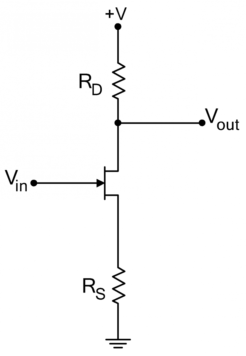
| Adding a drain resistor where Thus the gain of the amplifier is where the last equality assumes that the transconductance is high. |
 |
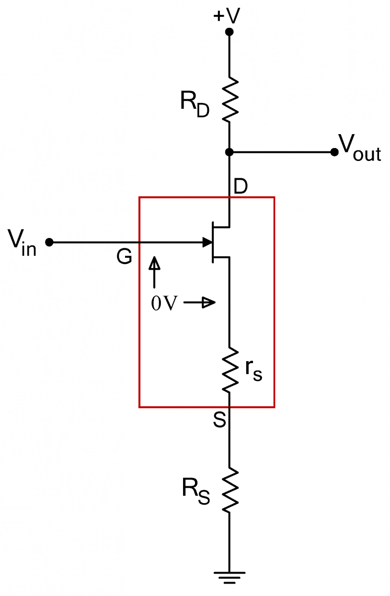 |
As with the source follower, the input current is given by the gate leakage current, so the amplifier’s input impedance is extremely high. The output impedance of the amplifier equals the drain resistance RD , and unlike the output impedance in the follower circuit, it is not low.
Differential Amplifiers
| Differential amplifiers have two inputs, V+ and V-, and one or two outputs. In an ideal differential amplifier, the amp’s output depends solely on the difference between the two inputs, |
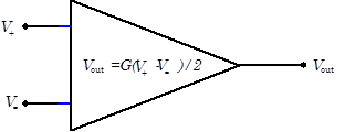 |
Differential amplifiers are one of the most common building blocks in analog circuit design. The front end of every op amp, for example, consists of a differential amplifier. Differential amplifiers are used whenever a desired signal is the difference between two signals, particularly when this difference is masked by common mode noise.
Electrocardiograms are an example of the use of differential amplifiers. The heart generates electrical signals, which can be detected by electrodes placed against the skin, but the signal from a single electrode would be swamped by background pickup; as you know from touching the input to an oscilloscope, the body is an excellent antenna for noise in frequencies ranging from 60Hz to 100MHz . Fortunately these undesired signals are nearly equal everywhere on the body. By using two pickups, placed so that the signal from the heart has the opposite sign on the pickups, and amplifying the difference between the two pickups with a differential amplifier, the desired signal from the heart can be preferentially amplified over the unwanted noise.
| Differential amplifiers are constructed from a matched pair of transistors as shown to the right. The two inputs are on the gates of the transistors. The drain of either transistor can be used as the output; in some cases both JFET drains are used to provide a differential output, i.e outputs of opposite phase. | 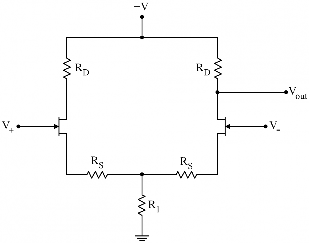 |
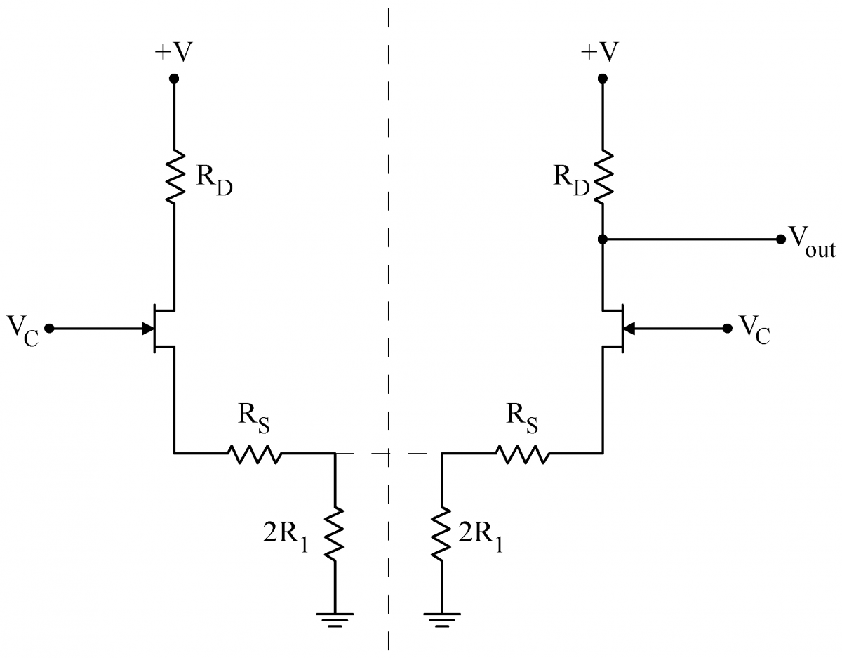
| When driven with a common mode signal only, symmetry tells us that both sides of the circuit will behave identically. In this case, we can pretend to split the circuit down the middle, as shown at right. The two We can use Eq. (1) to calculate the gain of the two halves of the circuit individually. This common mode gain is minus one times the following: In practice, the common resistor |
 |
| The response of the two transistors to a small differential signal Since the two sides of the circuit are only connected at place hed at constant voltage by the conceptual battery, the two sides effectively decouple. Then Eq. (1) yields the differential gain (two factors of -1 result in a +1 here) If we choose the drain resistors, Thus, we have accomplished our goal: a large differential gain (Eq. (3)) and a small common mode gain (Eq. (2)). |
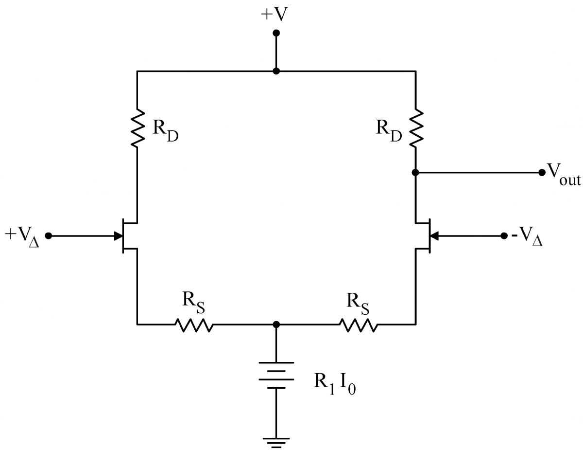 |
The circuit is linear. Consequently for any particular V+ and V− , the output will be the sum of the outputs for the corresponding VΔ and VC . A not uncommon case occurs with an input signal is applied to just one input, say V+ , and the other input (V− ) is grounded. Then, VΔ=V+/2 and VC=V+/2 as well. (Note how V−=VC−VΔ=0 ) The gain for this single input will be half the differential gain: RD/2(RS+rs) .
JFET Linearized Resistor
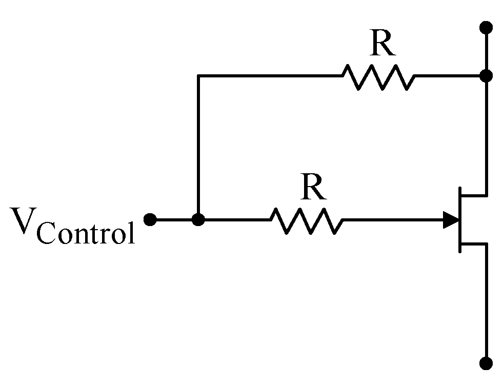
| JFET's can be used as variable resistors. IMPORTANT NOTE: The lower resistor R in the diagram at right is in the wrong location; the correct location is shown in Problem 5.8. In this application, the drain source resistance where The linearity between Note that this is an application of a JFET being used in the somewhat unusual linear regime as opposed to the more common saturated regime. |
 |
Parasitic Oscillations
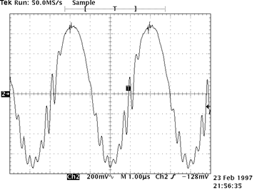
| Parasitic oscillations are unwanted, high frequency oscillations usually caused by unintended positive-feedback loops. The loops are closed by unintended capacitative coupling between two neighboring wires. Because the oscillations normally occur at very high frequencies (1 to 100 MHz), capacitances of only a few picofarads are sufficient to cause oscillations. Parasitic oscillations often first appear as “hair” on an otherwise undistorted signal. For example, in the scope trace on the right, the small oscillations at the top of the original sine wave are due to parasitic oscillations. | 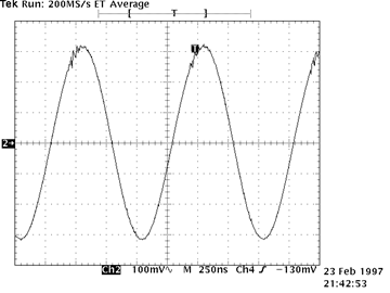
Minor Parasitic Oscillations
|
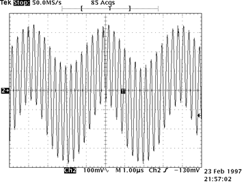
| Larger parasitic oscillations may cover a substantial fraction of the signal, as shown to the right, or they may completely dominate the signal, as shown at the extreme right. Touching the circuit, or even waving your hand near the circuit, can either accentuate or suppress the oscillations. Parasitic oscillations generally, but not always, require circuits with gain. The followers that we built in last week’s lab were relatively immune from oscillating, but the amplifiers that you are building this week will likely exhibit paras |
Significant Parasitic Oscillations
Disasterous Parasitic Oscillations
 |
There are no hard and fast rules for eliminating parasitic oscillations, but clean circuit layout goes a long way. Keep your leads short and un-jumbled. Lay your signals out from left to right, and keep large output signals away from small input signals. Believe it or not, beautifully wired circuits work better!
Unfortunately not even clean circuit layouts will always suppress the oscillations. At very high frequencies, the internal capacitances inside components, aided by the inductances formed by the component leads, can cause oscillations. An additional feedback route is through the power supplies themselves. Frequently parasitic oscillations can be tamed by liberally adding “decoupling” capacitors across the power supply. The decoupling capacitors function by providing a low impedance path to ground at high frequency, thereby shorting out the high frequency oscillations. To be effective, decoupling capacitors should placed close to the circuit components. Try placing 0.1μF capacitors between +12V and ground, –12V and ground, and between +12V and –12V. Vary the locations of the capacitors, and use more than one, until the oscillations go away. Don’t be greedy; a 1 or 10μF capacitor will not work better than a 0.1μF capacitor. In fact, the larger internal inductances of large capacitors may well make them work worse than smaller capacitors. This is particularly true of electrolytic capacitors.
When power supply decoupling capacitors are insufficient, placing a small capacitor across the input of a circuit will sometimes work.
Packaging and Leads
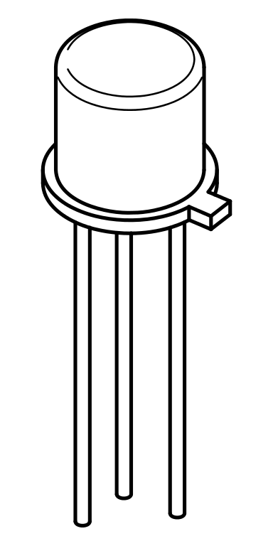
| Transistors are manufactured in many different packages and sizes. Our 2N4392 JFETs come in a metal can. (Devices starting with 1N are always diodes; devices starting with 2N are always transistors.) As with many devices, the lead diagram depends on the view. A bottom view (immediate right) looks at the device from the lead side. A top view (center right) looks at the device from the non-leaded side. The 2N4392 leads are arranged in a triangle; the gate lead is the first lead clockwise from the tab when looked at in a top view. When inserting the JFET into the breadboard, there is no need to squash the leads out horizontally. In fact, doing so will risks accidentally shorting the JFET leads to the metal case. Instead of squashing the leads, just bend them out gently so that they form a triangular pattern, and are in different columns on the breadboard. It may be useful to have one of the leads span the breadboard's narrow socketless row region. |
 2N4392 2N4392Bottom View |
Top View
|
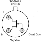 |
| Many JFETs, including the 2N4392, are symmetrically constructed. The source and drain can be exchanged without changing the device behavior. But for simplicity, use should generally use the correct source and drain leads. Asymmetric JFETs, in which the source and drain cannot be exchanged, are normally drawn with an offset gate lead as shown at right. |
 |