Friday, 20 September 2019

Differential amplifier using JFET

Pre-lab

1.     Explain in detail how a signal applied to the gate of one transistor in a differential amplifier can produce an output on the drain of the other transistor.
2.     What are parasitic oscillations? How do you minimize them?
Do not forward bias the JFET gates. Forward gate currents larger than 50mA will burn out the JFETs!


The Laboratory Staff will not help debug any circuit whose power supplies have not been properly decoupled!

Background

Voltage Amplifiers
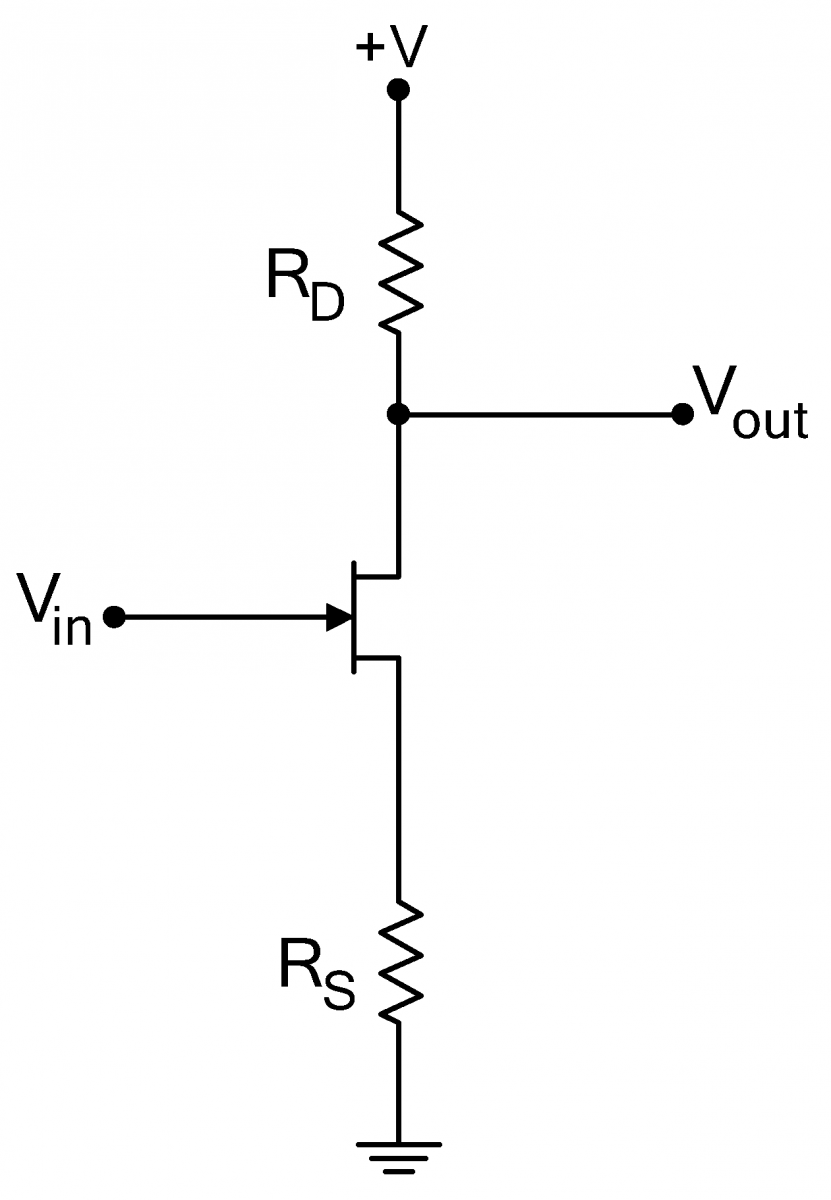
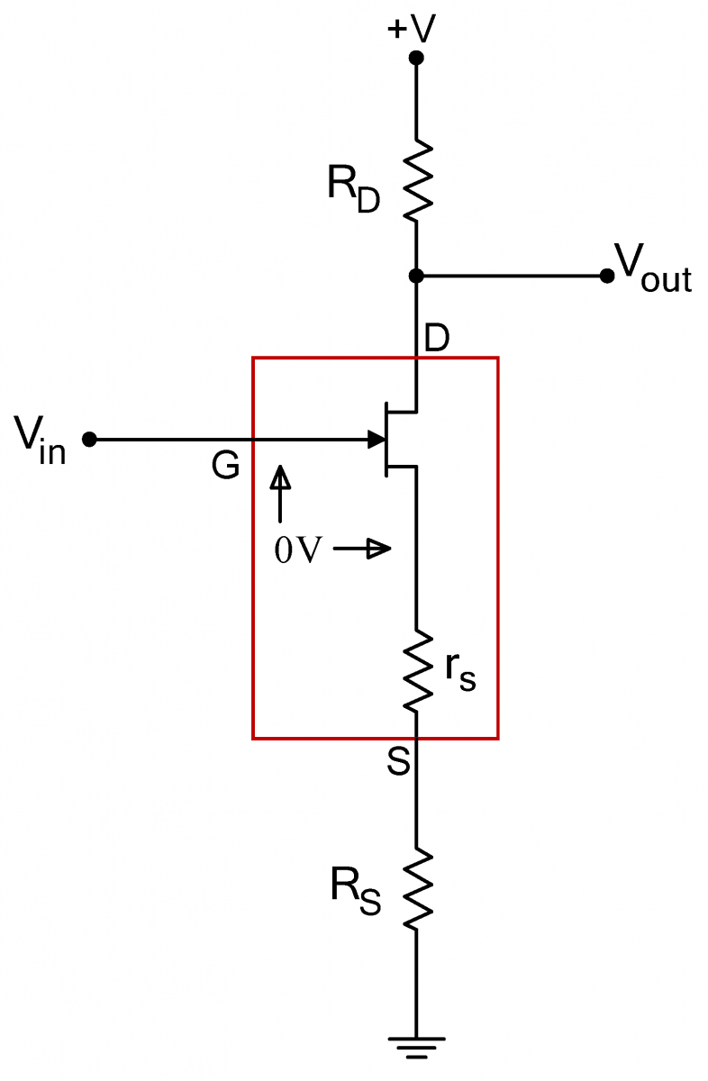
Adding a drain resistor RD to a source-follower turns it into a voltage amplifier, as shown to the right. This topology amplifier is known as a common source amplifier The equivalent small signal circuit for the amplifier is shown to the extreme righnt and is most easily understood by remembering that the current in a source follower is given by
is=vinRS+rs.
where rs=1/gm. Since this current is unchanged by the addition of the drain resistor, the output voltage will be
vout=RDis=RDRS+rsvin.
Thus the gain of the amplifier is
G=RD/(RS+rs)RD/RS,            (1)
where the last equality assumes that the transconductance is high.

JFET Amp0.png JFET Amp00.png
As with the source follower, the input current is given by the gate leakage current, so the amplifier’s input impedance is extremely high. The output impedance of the amplifier equals the drain resistance RD, and unlike the output impedance in the follower circuit, it is not low.
 Differential Amplifiers
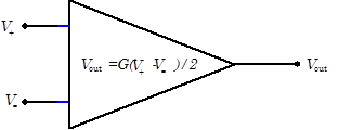
Differential amplifiers have two inputs, V+ and V-, and one or two outputs. 
In an ideal differential amplifier, the amp’s output depends solely on the difference between the two inputs,
VΔ=(V+V)/2, namely Vout=GVΔ. Unfortunately, the output of any real differential amplifier also depends weakly on the average of the two inputs. This average, VC=(V++V)/2, is called the common mode of the amp.
Differential amplifiers are one of the most common building blocks in analog circuit design. The front end of every op amp, for example, consists of a differential amplifier. Differential amplifiers are used whenever a desired signal is the difference between two signals, particularly when this difference is masked by common mode noise.
Electrocardiograms are an example of the use of  differential amplifiers. The heart generates electrical signals, which can be detected by electrodes placed against the skin, but the signal from a single electrode would be swamped by background pickup; as you know from touching the input to an oscilloscope, the body is an excellent antenna for noise in frequencies ranging from 60Hz to 100MHz. Fortunately these undesired signals are nearly equal everywhere on the body. By using two pickups, placed so that the signal from the heart has the opposite sign on the pickups, and amplifying the difference between the two pickups with a differential amplifier, the desired signal from the heart can be preferentially amplified over the unwanted noise.
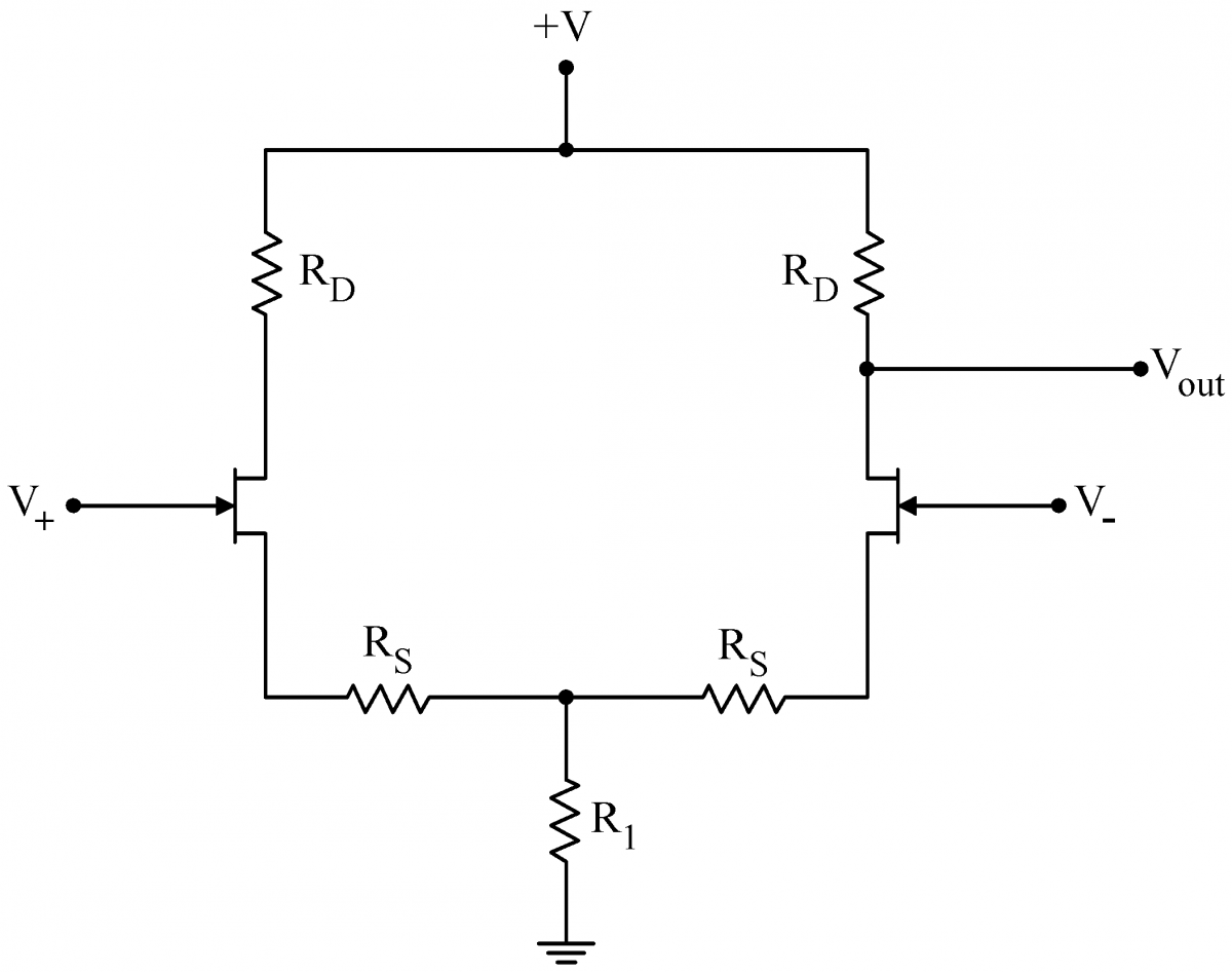
Differential amplifiers are constructed from a matched pair of transistors as shown to the right.  The two inputs are on the gates of the transistors.  The drain of either transistor can be used as the output; in some cases both JFET drains are used to provide a differential output, i.e outputs of opposite phase. Differential Generic.png
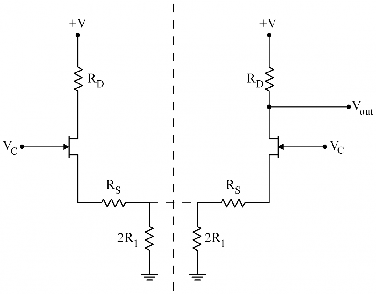
When driven with a common mode signal only, symmetry tells us that both sides of the circuit will behave identically.  In this case, we can pretend to split the circuit down the middle, as shown at right.  The two 2R1 resistors combine to make the original R1.  Symmetry requires that the two upper ends of the 2R1 resistors be at the same potential; thus no current would flow in the dashed line that connects the two ends.  Since there is no current, we can pretend that the resistors are disconnected.
We can use Eq. (1) to calculate the gain of the two halves of the circuit individually.  This common mode gain is minus one times the following:
RD2R1+RS+rs      (2)

In practice, the common resistor R1 is always made much greater than the source resistors, so the gain reduces to Rd/2R1. Further, R1 is always chosen to be much larger than the drain resistor RD. Consequently, the gain for  common mode signals is low and these signals are strongly attenuated.
Differential Common Mode.png
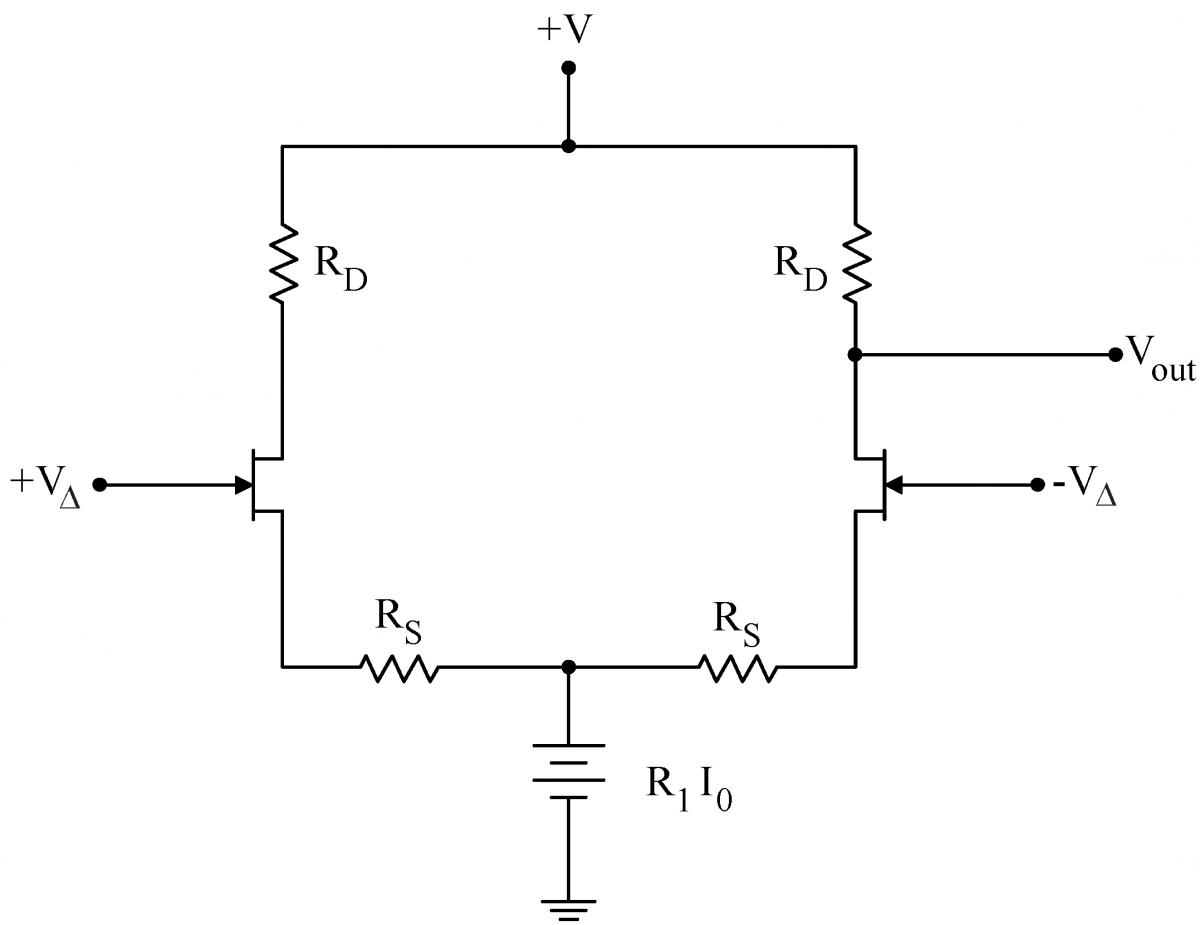
The response of the two transistors to a small differential signal VΔ, on the other hand, will be equal and opposite. If the current through the left JFET increases (V+>0), the current through the right JFET will decrease by an equal and opposite amount. The net current flow I0 through, and voltage drop across, the common resistor will not change with VΔ. Consequently the common resistor can be replaced with a conceptual voltage source of strength R1I0, as depicted at right.
Since the two sides of the circuit are only connected at place hed at constant voltage by the conceptual battery, the two sides effectively decouple.  Then Eq. (1) yields the differential gain (two factors of -1 result in a +1 here)
RDRs+rs        (3)
If we choose the drain resistors, RD, to be large compared to the source resistors RS, then the differential gain will be large.
Thus, we have accomplished our goal:  a large differential gain (Eq. (3)) and a small common mode gain (Eq. (2)).
Differential Differential Mode.png
The circuit is linear.  Consequently for any particular V+ and V, the output will be the sum of the outputs for the corresponding VΔ and VC.  A not uncommon case occurs with an input signal is applied to just one input, say V+,  and the other input (V) is grounded. Then, VΔ=V+/2 and   VC=V+/2 as well.  (Note how V=VCVΔ=0)  The  gain for this single input will be half the differential gain: RD/2(RS+rs).
JFET Linearized Resistor
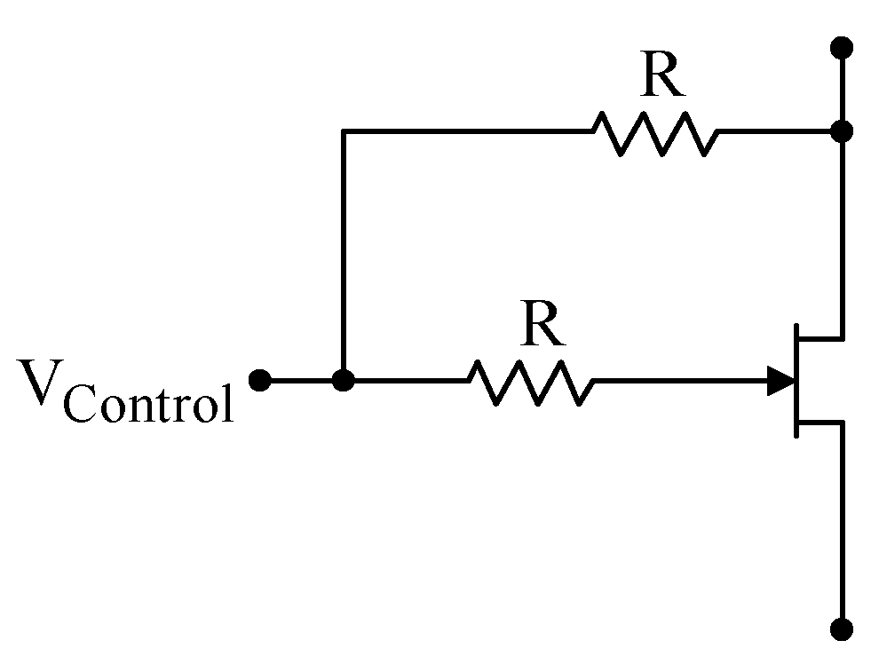
JFET's can be used as variable resistors.  IMPORTANT NOTE: The lower resistor R in the diagram at right is in the wrong location; the correct location is shown in Problem 5.8.   In this application, the drain source resistance RDS can be controlled by a voltage, VControl, applied to the gate.  With just a JFET, however, this resistance is dependent on the VDS, and the "resistor" is nonlinear.  It can be shown that the linear-regime resistance RDS between a JFET’s drain and source is given by
1RDS=2k[(VGSVP)VDS/2],
where k is a parameter that depends on the individual JFET, VP is the voltage where the JFET first conducts (the pinch-off, cutoff, or threshold voltage), and VDS is the voltage between the drain and the source. 
The linearity between VDS and ID can be restored by adding a signal equal to VDS/2 to the gate. This can be done by adding two resistors to the gate circuit as shown to the right.  This circuit functions as an excellent variable resistor.
Note that this is an application of a JFET being used in the somewhat unusual linear regime as opposed to the more common saturated regime.
Generic Attenuator.png
Parasitic Oscillations
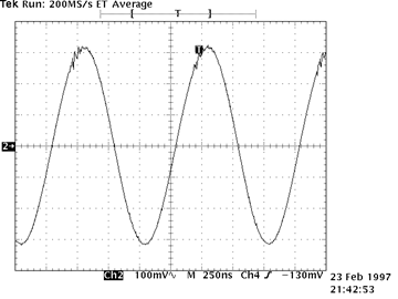
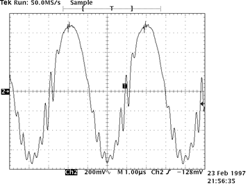
Parasitic oscillations are unwanted, high fre­quency oscillations usually caused by unintended positive-feedback loops. The loops are closed by unintended capacitative coupling between two neighboring wires. Because the oscillations normally occur at very high frequencies (1 to 100 MHz), capacitances of only a few picofarads are sufficient to cause oscillations.  Parasitic oscillations often first appear as “hair” on an otherwise undistorted signal. For example, in the scope trace on the right, the small oscillations at the top of the original sine wave are due to parasitic oscillations.
Minor Parasitic Oscillations
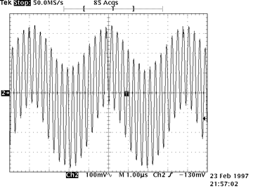
Larger parasitic oscillations may cover a substantial fraction of the signal, as shown to the right, or they may completely dominate the signal, as shown at the extreme right.
Touching the circuit, or even waving your hand near the circuit, can either accentuate or suppress the oscillations.
Parasitic oscillations generally, but not always, require circuits with gain. The followers that we built in last week’s lab were relatively immune from oscillating, but the amplifiers that you are building this week will likely exhibit paras
image015.png 
Significant Parasitic Oscillations

Disasterous Parasitic Oscillations


There are no hard and fast rules for eliminating parasitic oscillations, but clean circuit layout goes a long way. Keep your leads short and un-jumbled. Lay your signals out from left to right, and keep large output signals away from small input signals. Believe it or not, beautifully wired circuits work better!
Unfortunately not even clean circuit layouts will always suppress the oscillations. At very high frequencies, the internal capacitances inside components, aided by the inductances formed by the component leads, can cause oscillations. An additional feedback route is through the power supplies themselves. Frequently parasitic oscillations can be tamed by liberally adding “decoupling” capacitors across the power supply. The decoupling capacitors function by providing a low impedance path to ground at high frequency, thereby shorting out the high frequency oscillations. To be effective, decoupling capacitors should placed close to the circuit components. Try placing 0.1μF capacitors between +12V and ground, –12V and ground, and between +12V and –12V. Vary the locations of the capacitors, and use more than one, until the oscillations go away. Don’t be greedy; a 1 or 10μF capacitor will not work better than a 0.1μF capacitor. In fact, the larger internal inductances of large capacitors may well make them work worse than smaller capacitors. This is particularly true of electrolytic capacitors.
When power supply decoupling capacitors are insufficient, placing a small capacitor across the input of a circuit will sometimes work.

 Packaging and Leads
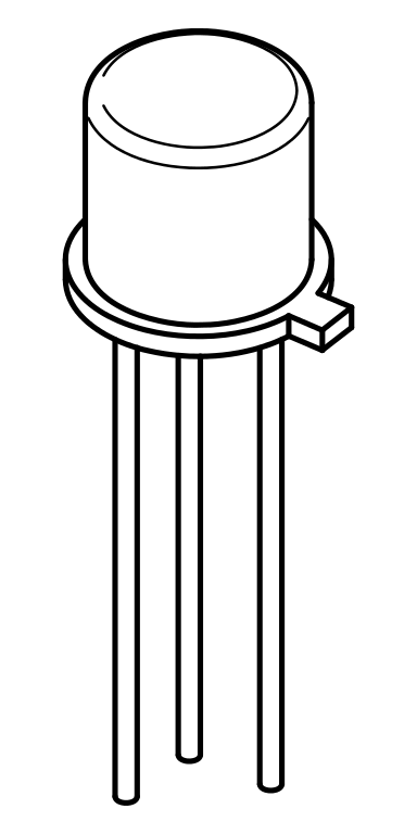
Transistors are manufactured in many different packages and sizes. Our 2N4392 JFETs come in a metal can. (Devices starting with 1N are always diodes; devices starting with 2N are always transistors.)
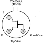
As with many devices, the lead diagram depends on the view.  A bottom view (immediate right) looks at the device from the lead side.  A top view (center right) looks at the device from the non-leaded side.
The 2N4392 leads are arranged in a triangle; the gate lead is the first lead clockwise from the tab when looked at in a top view.
When inserting the JFET into the breadboard, there is no need to squash the leads out horizontally. In fact, doing so will risks accidentally shorting the JFET leads to the metal case.
Instead of squashing the leads, just bend them out gently so that they form a triangular pattern, and are in different columns on the breadboard.  It may be useful to have one of the leads span the breadboard's narrow socketless row region.
 2N4392
Bottom View
TO-18.png
Top View
Many JFETs, including the 2N4392, are symmetrically constructed. The source and drain can be exchanged without changing the device behavior. But for simplicity, use should generally use the correct source and drain leads.
Asymmetric JFETs, in which the source and drain cannot be exchanged, are normally drawn with an offset gate lead as shown at right.


Thursday, 19 September 2019

Daily updates 19 September 2019

National

1. GoI inaugurates 15 power projects in Jammu & Kashmir

  • Union Minister of State for Power RK Singh and Jammu and Kashmir Governor Satya Pal Malik have jointly inaugurated 15 power projects.
  • They also laid the foundation stone for 20 other different Centrally-sponsored schemes in Srinagar.
  • Under a scheme, 1 lakh LED (light-emitting diode) street lights will be installed in Srinagar city, saving ₹29 crores annually to the Srinagar Municipal Corporation. The government is working to ensure 24 hours electricity supply to all the citizens of the country, including in Jammu and Kashmir, and Ladakh region.

2. International Workshop for National Water Museum

  • The Jal Shakti Ministry is planning to develop a National Water Museum to increase awareness among people on the conservation of the natural resource.
  • The Jal Shakti Ministry is also organising an International Workshop which will be attended by experts from India and abroad.
  • The outcome of the workshop will be a blueprint for establishing the proposed National Water Museum under the aegis of Jal Shakti Ministry.
  • During the workshop, possible broad composition, the content of the museum including highlighting importance of water and its current state in different regions of the country, possible solutions, traditional and modern water management practices and localised success stories are proposed to be discussed.

Static/Current Takeaways Important For RRB NTPC/IBPS RRB Mains:

  • Union Minister of Jal Shakti: Gajendra Singh Shekhawat.

3. India Post expands speed post service to 6 new foreign countries

  • India Post expanded speed post service to six new foreign destinations in Asia, Europe and South America.
  • The Department of Posts has announced commencing of International Speed Post (EMS) Service to Bosnia and Herzegovina, Brazil, Ecuador, Kazakhstan, Lithuania and North Macedonia.
  • EMS or Express Mail Service is a premium service that enables its users to send documents and merchandise faster and with the added facility of being able to track the movement of the item on the internet.
  • This facility is expected to augment people to people contact with these countries and foster trade as EMS is a popular channel for small and medium enterprises.
  • The EMS service to these countries will henceforth be available at major Post offices across India.

Static/Current Takeaways Important For RRB NTPC/IBPS RRB Mains:

  • Secretary, Department of Posts & Chairperson, Postal Services Board: Ananta Narayan Nanda.
  • Headquarters: New Delhi; Founded: 1 April 1854.
  • Director-General: Meera Handa.

State News

4. Delhi Police's launches Tatpar app for citizen-centric servicesr

  • Delhi Lieutenant Governor Anil Baijal launched 'Tatpar' app, developed by the Delhi Police, which is a one-stop destination for access to over 50 citizen-centric services.
  • The app amalgamates all the websites and mobile applications of Delhi Police, and over 50 services which can now be accessed with a single touch in the app.
  • Through the app, citizens can navigate to their nearest police station, traffic pit and prepaid taxi booth. On a single touch, the user will be provided with the directions as well as the complete contact details of the concerned Station House Officer (SHO) of a police station.

Static/Current Takeaways Important For IBPS RRB Main 2019:

  • Chief Minister of Delhi: Arvind Kejriwal

Appointment

5. ADB president Takehiko Nakao resigns

  • Asian Development Bank (ADB) President Takehiko Nakao has announced his resignation. He became the president of ADB on April 28, 2013.
  • He expanded the operations of the funding agency from USD 14 billion in 2013 to USD 22 billion in 2018.
  • He also ushered in the merger of Ordinary Capital Resources and concessional lending operation of the Asian Development Fund (ADF) and steered the launch of ‘Strategy 2030.
  • The new president will be elected in accordance with an open, transparent and merit-based procedure.

Static/Current Takeaways Important For IBPS RRB Main 2019:

  • Headquarters of ADB: Manila, Philippines; Founded:19 December 1966.
  • Member of ADB: 68 countries.

6. GoI Appoints Four Supreme Court Judges

The Centre has cleared four names recommended by the Supreme Court Collegium for elevation as judges of the apex court. The four appointed judges are

  • Himachal Pradesh High Court: Chief Justice V. Ramasubramanian
  • Punjab and Haryana High Court: Chief Justice Krishna Murari
  • Rajasthan High Court: Chief Justice S. Ravindra Bhat
  • Kerala High Court: Chief Justice Hrishikesh Roy

The Supreme Court vacancies had increased its judicial strength from 31 to 34 following the enactment of the Supreme Court (Number of Judges) Bill of 2019.

Static/Current Takeaways Important For RRB NTPC/IBPS RRB Mains:

  • Chief Justice of India: J Ranjan Gogoi; Founded: 26th January 1950.

7. Robert O'Brien becomes National Security Adviser of US

  • Robert O'Brien has been appointed as the National Security Adviser of United States of America.
  • Robert O'Brien will replace John Bolton as the NSA of US.
  • Robert O'Brien has had a long career in foreign policy working for both main US parties and currently heading the hostage negotiations at the State Department.

Static/Current Takeaways Important For IBPS RRB Clerk Mains:

  • US President: Donald Trump; Capital: Washington, D.C; Currency: US Dollar.

Ranks and Reports

8. Indian diaspora largest in the world at 17.5 million: UN Report

The International Migrant Stock 2019 was released by the Population Division of the UN Department of Economic and Social Affairs (DESA). The report provides the latest estimates of the number of international migrants by age, sex and origin for all countries and areas of the world.

As per the report, India was the leading country of origin of international migrants in 2019 with a 17.5 million strong diaspora.

Some important findings of the report:

  • The top 10 countries of origin account for one-third of all international migrants. India is the leading country of origin of international migrants with 17.5 million persons living abroad. Migrants from Mexico constituted the second largest diaspora (11.8 million), followed by China (10.7 million).
  • Europe hosted the largest number of international migrants (82 million), followed by Northern America (59 million) and Northern Africa and Western Asia (49 million). India hosted 5.1 million international migrants in 2019.
  • Among the international migrants in India, the female population was 48.8% and the median age of international migrants was 47.1 years.
  • In India, the highest number of international migrants came from Bangladesh, Pakistan and Nepal.
  • In terms of age, one out of every seven international migrants is below the age of 20 years.

Static/Current Takeaways Important For IBPS RRB PO Mains:

  • UN Under Secretary General for Department of Economic and Social Affairs: Liu Zhenmin.

Awards

9. Anand Kumar felicitated with Education Excellence Award 2019

  • Super 30 founder and noted mathematician Anand Kumar has been felicitated in the US with a prestigious Education Excellence Award 2019.
  • The Foundation For Excellence (FFE) awarded him on the occasion of the organisation's 25th anniversary.
  • Anand has been running a highly innovative Super 30 programme for the last 18 years. He mentors 30 students free off cost through a year-long residential coaching for India's premiere IIT-JEE.

Summit and Conferences

10. Home Minister chair the meeting of Northern Zonal Council in Chandigarh

  • Union Home Minister Amit Shah will chair the 29th meeting of the Northern Zonal Council.
  • The grouping comprises states of Haryana, Himachal Pradesh, Punjab and Rajasthan besides union territories of Jammu and Kashmir, Ladakh and the National Capital Territory of Delhi. The Haryana chief minister Manohar Lal Khattar is the vice-chairman and host of the meeting.
  • The zonal councils discuss a broad range of issues, including boundary disputes, security, infrastructure-related matters such as roads, transport, industries, water and power besides matters pertaining to forests and environment, housing, education, food security, tourism and transport.
  • Five zonal councils were set up in 1957 under the States Reorganisation Act, 1956. The Union home minister is the chairman of each of these five councils.

Defence

11. Rajnath Singh becomes 1st Defence Minister to fly in LCA Tejas

  • Defence Minister Rajnath Singh becomes the first defence minister to fly in the indigenously-built light combat aircraft (LCA) Tejas. He flew in the Tejas fighter aircraft from the HAL airport in Bengaluru.
  • Defence Minister was accompanied by Air Vice Marshal N Tiwari, who is also the Project Director, National Flight Test Centre, ADA (Aeronautical Development Agency) in Bengaluru.

Sports

12. Anurag Thakur announces cricket and sports academy for Leh

  • Union Minister of State for Finance and Corporate Affairs Anurag Thakur announced that a cricket and sports academy will be set up in Leh, Ladakh.
  • This cricket and sports academy will ensure that talented athletes of the region get the required training to excel. He also joined Army personnel in Leh to carry out a cleanliness drive to mark Prime Minister Narendra Modi's 69th birthday.

13. Vinesh Phogat wins bronze medal in Wrestling World Championships

  • Vinesh Phogat won the bronze medal at the Wrestling World Championships held in Nur-Sultan, Kazakhstan.
  • She defeated Maria Prevolaraki of Greece in the 53 kg freestyle event.
  • Vinesh Phogat has also won India an Olympic quota in the 53 kg freestyle event of Tokyo Olympics.

Obituaries

14. Veteran Malayalam Actor Sathar Passes Away

  • Veteran Kerala actor Sathar passed away. He made his acting debut in 1975 with Malayalam movie Bharyaye Aavashyamundu directed by M. Krishnan Nair & in 1976 with Vincent Master’s directorial Anavaranam. He was acted in more than 300 films, majority of them in Malayalam.

Miscellaneous

15. Beijing 2022: Paralympic and Olympic mascots unveiled

  • A smiling panda and a walking Chinese lantern will be the mascots for the 2022 Winter Olympics and Paralympics in Beijing, China.
  • The mascots were revealed at a ceremony at the Shougang Ice Hockey Arena in the Chinese capital.
  • The mascot, named Bing Dwen Dwen, is a chubby giant panda wearing a suit of ice was revealed as the official mascot for Beijing Winter Olympics 2022.
  • Chinese lantern Shuey Rhon Rhon was declared as the official mascot for Winter Paralympics 2022.

Static/Current Takeaways Important For RRB NTPC/IBPS RRB Mains:

  • President of China: Xi Jinping; China Capital: Beijing; Currency: Renminbi.